CNSI became interested in Microfluidics devices constructed from COC (Cyclic olefin copolymer) because they are not only optically transparent, but also X-ray and UV transparent. As BioPacific is planning on procuring a powerful X-ray microscope, the need for an alternative to PDMS constructed microfluidics devices that are X-ray transparent sparked our interest in COC. The difficulty with COC's however is that they are much more difficult to bond, and unlike PDMS are unable to be used in a mold at room temperature. This page will cover and outline many of the attempts and results of my research into the bonding and manufacturing of COC devices.
Intro
COC also known as cyclic olefin copolymer is a thermoplastic used in microfluidic devices as well as food/body safe packaging. COC is often utilized due to its resistance to polar solvents, biocompatibility, and UV/X-ray transparency. Therefore it is the perfect material for microfluidic devices containing bacteria or that need to be imaged outside the visible spectrum. As TOPAS is the sole producer of COC and only sells through exclusive distributors, small quantities of COC can be difficult to obtain after exhausting supplier samples. Several different grades of COC are available, with the main difference being the glass transition temperature of the material. TOPAS 6013M-07 and 8007X-04 with Tg of 142° and 78° respectively were used for testing.
Fabrication Options
The construction of COC microfluidic devices often utilize two or more COC “plaques” (≥ 1mm) or films (≤ 1mm) bonded together to form a completed microfluidic “chip”. There are two main methods of which to form a permanent bond between COC substrates; the first utilizes cyclohexane to slightly dissolve the surface of the COC in a process known as solvent bonding, and the second method involves heating the substrates above or close to the glass transition temperature (Tg) while pressure is applied in a process known as thermal bonding.
Solvent Bonding
Solvent bonding requires the use of a strong non polar solvent (preferably an organic hydrocarbon) such as cyclohexane or toluene which can penetrate the surface of the COC and allow for jamming of the solvent spaced polymer chains when pressed together. The advantage of solvent bonding is that only one substrate needs to be exposed to cyclohexane which allows for immobilized bacteria to be patterned on the COC that is not exposed to solvent without risking denaturing the bacteria. Solvent bonding is performed at room temperature and requires less pressure to be applied to the chip (arox. 20 psi), resulting in less deformation of the channel within the chip. Care must be taken to apply even pressure across the entire chip to prevent bubbles from forming during the bonding process. The solution of cyclohexane must also be diluted with acetone within a narrow window (centered at 35-40 wt% cyclohexane) to prevent over penetration of the solvent causing pitting and worse optical clarity. Solvent bonding is also incompatible with laser cutting or heat polishing of the COC unless the substrate is annealed after cutting. Exposure of a non annealed laser cut surface will result in rapid crazing of the COC and worse optical clarity.
Thermal Bonding
Thermal bonding uses heat and pressure to fuse two or more COC substrates together and can be done both above and just below Tg. Bonding below Tg is often preferred as it results in less distortion of the channels within the chip, however it requires more time and results in a less strong bond. After cleaning in ozone, a hot press was used to both regulate the temperature of the bonding surface as well as apply pressure down upon the chip. Similar to solvent bonding, care must be taken to apply even pressure across the entire chip in order to get a consistent and transparent bond. During the bonding process the COC takes up the texture of the hot plates on both sides, therefore using polished aluminum plates over the press jaws results in a smoother surface finish which scatters fewer electromagnetic waves.
Channel Construction
There are several methods by which the channels can be created within the COC chip. A three layer chip can be created using a bottom plate, midplate containing through channels, and a lid containing the inlet and outlet ports. This method allows for the channels to be laser cut or machined completely through the COC film or plaque which results in no optical distortion from the midplate while imaging the channel. As mentioned earlier, laser cutting channels requires annealing the COC below Tg for at least 2 hours if solvent bonding is utilized to avoid crazing of the material when exposed to cyclohexane. Another possibility is to emboss or pressure mold the channel within the bottom plate itself, and affix a lid containing inlet and outlet ports. This method has the advantage of reducing the number of joints and bonds within the chip, but requires care to ensure that the floor of the channel is polished to avoid scattering electromagnetic waves. A three layer chip has the advantage of being easier to polish as there is no recessed channel such as the one present in two layer embossed, molded, or machined chips. Pressure molding or embossing also has the disadvantage of requiring a “die” or mold to be made for each chip geometry and any scratch present on the die will transfer to the COC substrate when pressure is applied. Pressure molding is done above the melting point of the COC (200° C), whereas embossing is done at slightly above the Tg of the material (110° C). Care should be taken when machining and polishing the die to avoid unnecessary post processing and channel deformation stemming from polishing the COC after patterning. Machining of the COC itself can also be used to construct through or partial channels within COC plaque. This method is limited to the diameter of endmills and the effective clearing of chips and removal of heat to prevent the substrate from melting under cutting loads.
Final Considerations
As X-ray intensity decays exponentially with the thickness of the material so it is pertinent to keep material thickness above and below the channel to a minimum. For this reason it is preferable to use 240 micron COC film for the top and bottom of a through channel chip (or just the top for a 2 layer chip). Using 6013M-07 film for the top and bottom and 8007X-04 for the channel plate in conjunction with thermal bonding leads to almost no optical distortion as the 6013M-07 film does not deform due to the applied heat and the 8007X-04 channel plate is able to bond to the thin film while experiencing minimal distortion by being heated just below its Tg.
Experimental Results
Chips were created through solvent or thermal bonding and channels were created by laser cutting, hot embossing, pressure casting, or machining. Overall thermal bonding resulted in the most consistent and optically transparent bonding, however the risk of deforming channels during thermal bonding (even below Tg) is much higher than that of solvent bonding. Machining the channels of a three layer chip also resulted in the best optical transparency as no polishing and minimal post processing is required.
Solvent Bonding
|
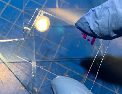
A process for solvent bonding has been established however it remains difficult to consistently achieve a consistent and optically transparent bond. Overpenetration of the cyclohexane as well as uneven bonding pressure often result in “bubbles” or pockets of reduced bonding/contact within the chip resulting in decreased optical clarity and strength. This can be minimized by pressing the chip between layers of thick PDMS to help apply even pressure across the entire surface. It was found that exposing the channel plate to cyclohexane rather than the lid(s) can increase optical clarity across the channel as any pitting will occur in the channel plate where the top and bottom of the channel itself is not exposed to cyclohexane.
|
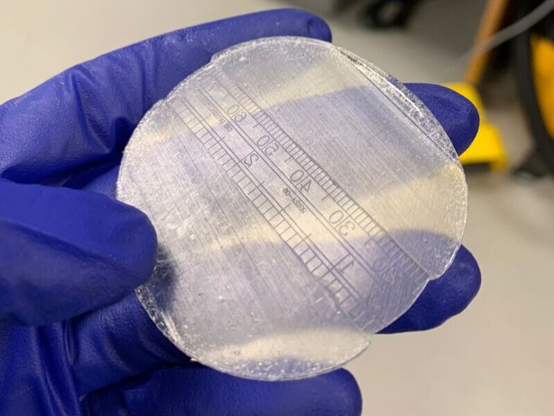
Best case optical quality of two samples of 240 micron COC film
|
Thermal Bonding
Thermal bonding has been used to create successful microfluidic devices with good transparency; however, care must be taken to avoid warping the lid(s) or channel plates. It was found that using 6013M-07 thin film for the lid(s) and 8007X-04 plaque or the channel plate reduces the chance of the lid(s) warping and entering the channel because of their higher Tg. This is pertinent for X-ray microscopy of COC as using thin film for the lid greatly increases X-ray transmission through the channel allowing for clearer imaging. Using thin film however reduces the usable pressure of the chip as under high fluid pressure the film will bulge out increasing the depth of the channel and beginning to break the thermal bond between film and plaque.
Thermal Embossing
|
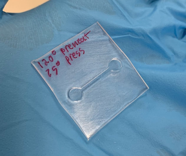
Thermal embossing shows promise as a method for creating 2 layer COC chips with high levels of optical clarity. Both the COC substrate and mold were heated to 110° C for 8007X-04 and once pressed the mold with COC substrate was allowed to cool and rest at 60° C while in the press before removal from the mold. Embossing has the advantage of being done below the melting point of 8007X-04 which greatly reduces the possibility of trapping bubbles within the mold during the embossing process. Polished plates and molds should be used to reduce the need to post process the chip. Embossing can lead to rounded corners at the surface of the channels, however this can be reduced by increasing the temperature of the COC substrate before placing it within the heated sides of the mold. Thermal embossing has the disadvantage of requiring a new mold to be created for each chip design, and any scratch on the master mold will transfer to every single chip created by said mold. On the other hand the consistency and lack of deburring stemming from thermal embossing makes it favorable for when more than a handful of chips is necessary.
|
An example of rounded corners requiring higher preheat of COC before pressing
|
Thermal Pressure Molding
|
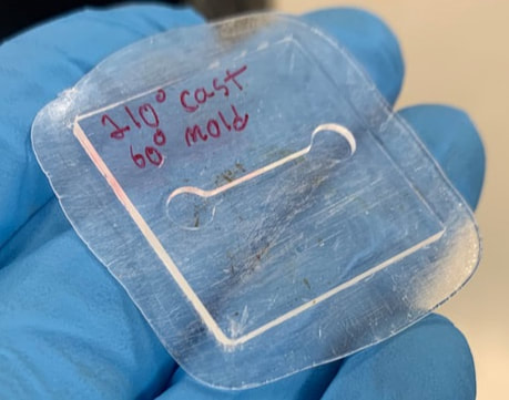
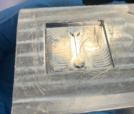
Result of thermal pressure molding
Thermal pressure mold
|
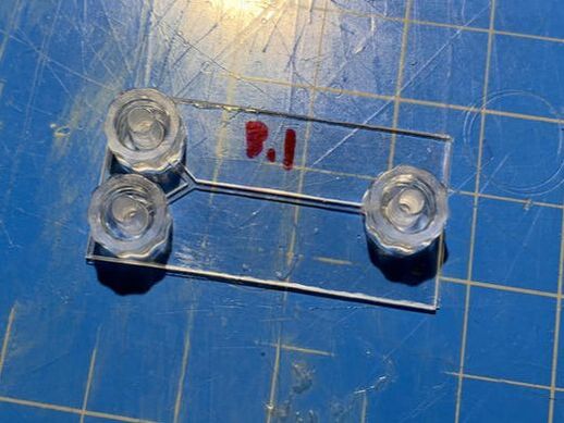
Thermal pressure molding has similar tradeoffs to thermal embossing although it occurs at much higher temperatures (above the melting point of the COC. Thermal pressure molding was done at 210° C for 8007X-04 and has a much higher likelihood of trapping air within the mold as raw COC pellets melted together to create the substrate. It was found that over-filling the mold and allowing considerable squeeze out greatly reduced the chances of bubbles becoming trapped within the important part of the substrate, however much more pressure is necessary for thermal pressure molding than embossing as surface area increases with squeeze out. During pressure molding the raw COC pellets and aluminum molds were heated on a hotplate to 210° C until the COC was a consistent moltant temperature. The COC was then transferred to the mold, and both sides of the mold were quickly moved to the press where several tons of pressure was applied. The mold was allowed to cool and rest at 60° C before the substrate was removed. In testing it was found that thermal pressure molding generated sharper corners and greater feature resolution than embossing. The tendency for the COC substrate to stick to the mold was much greater than embossing due to the exterior walls of the chip also being formed simultaneously. Mold release was used to facilitate the removal of substrate after forming.
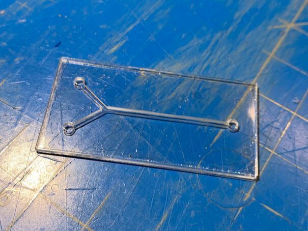
Example of high resolution (sub 50 micron features) thermal pressure molding of COC above its melting point.
|
Mold Options
Laser Cutting
Due to COC being a thermoplastic, laser cutting channels can be difficult due to the tendency of the laser to melt the base material. It was found that multiple passes reduces the amount of COC melted, however when cutting COC plaque or film deburring is required to allow consistent bonding. Laser cutting does allow the construction of channels in thin film down to at least 300 micron and smaller channels could probably be created with more fine tuning of the recipe. Because of the low Tg of both 8007X-04 and 6013M-07 laser cutting does create rounded edges on both the top and bottom of the COC and slag from the cut often sticks to the bottom edge of the COC film of plaque. This requires quite a bit of post processing to remove, and better wall finish can be achieved by machining the channels (at the cost of minimum channel thickness).
Machining
Machining COC is inherently more difficult than machining aluminium for the molds because COC is a low temperature thermoplastic: i.e. it melts and resolidifies around the tool when machining. Both 8007X-04 and 6013M-07 were machined, and both through channels and partial channels were made for three and two layer chips respectively. 6013M-07 is preferable for machining due to it higher Tg and can be machined dry; 8007X-04 is more difficult to machine due to its lower Tg leading to a tendency for the thermoplastic to resolidify around the tool and friction stir weld the material. Flood coolant and higher chip load per tooth (.0005) is necessary to remove heat from the 8007X-04 and facilitate chip removal. The raw machined finish leaves a bur on the wall that is conventionally milled, and a secondary finish path at final depth cleans up the surface finish considerably. Debring channels is necessary before bonding to prevent inconsistent bonding and the bottom surface of partial channels necessitates polishing as the machined surface would scatter too many electromagnetic waves. For this reason through channels are preferred as they require less post processing.
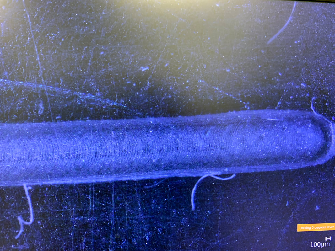
Example of a machined chip with 240 micron top and bottom lid
Polishing
Polishing partial channels was done with standard three part Novus plastic polishing compound. Mechanized polishing using wool polishing bits in a Dremel proved impractical due to the deformation of the wool bits resulting in only the center of the channel being polished. Instead, channels with a width to depth ratio of less than 2:1 were polished using the included polishing cloth and a sharpened wooden implement to drag the cloth along the bottom of the channel. Machined did not necessitate the use of Novus three (heavy scratch remover) and the polishing cloth was switched out between Novus two and Novus 1. Complete polishing of machined channels to reasonable optical transparency (able to easily distinguish 200 micron line spacing through channel floor) can be achieved with under 15 minutes of polishing for a straight 40 mm channel. For thin channel floors care must be taken not to deform the COC by applying too much pressure, and care should be taken to ensure that polishing cloth always covers the wooden implement to avoid scratching the channel while polishing. Sample was cleaned thoroughly between each polishing compound to avoid contamination and different polishing implements were used each time.
Sourcing and Materials
Due to the difficulty of obtaining COC, material selection and material on hand was dictated by the samples companies were willing to provide. As COC is typically used in industrial applications such as injection molding of shampoo bottles, the minimum order quantity is typically much larger than most labs could ever conceive of using. Raw 8007X-04 COC resin (pellets) were provided from PolyPlastics in 200 g sample baggies totaling 400 g with a minimum order quantity of 25 kg. ROHM provided several A4 sample sheets of EUROPLEX® 0F304 and 0F305 film in 1 mm and 240 micron thicknesses which are composed of PolyPlastics 8007X-04 and 6013M-07 respectively; minimum order quantities from ROHM is typically 340 mm by 100 m. Microfluidic chip shop based in Germany appears to be the only lab focused supplier of COC, however they do not do a good job of labeling the grade of COC their films or plaques are created from. 30 microscope slide plaques (25 mm x 75 mm x 1mm)
Next Steps
Going forward it is still unknown the effect of polishing on partial channels that are created using the hot press with either raw coc pellets or by embossing existing slides. Polishing is also yet to be employed on the die used to emboss or mold the channels and it is unknown how that will affect the amount of most processing necessary. Two sample chips are also going to be sent out to the X-ray lab as well as the researchers hoping to utilize COC chips for microfluidics to be run through some tests to validate the X-ray transparency as well as the flow characteristics of the chips. Other options such as laser cutting a PDMS midplate and compressing COC film on either side using a custom fixturing jig are also possibilities. This has the advantage of not necessitating any complicated or inconsistent bonding and being easy to change/modify the channel geometry, however it is still unknown how difficult maintaining even compression across then COC film will be and if the COC film will be able to consistently seal along the entire surface area shared with the PDMS.
